
Alex Lapayev. Analog Input/Output Compensated.3. Analog Input and Output Compensated Schematics. PracticeI think it would be fair to start describing applied devices with the presentation of the very first scheme, which uses the above-mentioned principle of compensation. As it was mentioned above, in the late nineties of the past century I faced a challenging task. We needed a brand new input-output analog driver for city telecom stations. We needed a driver that could provide an exceptionally clear reception and transmission of audio information at long distance (up to 20 km) by means of a common bidirectional line. The situation was aggravated by transmission of both audio signals and signals managing negative voltage of several volts. For correct functioning of hybrid systems and noise protection, receivers and transmitters schemes should have equal and quite evident impedance and should be in compliance with the communication line. The size of devices also meant a lot. Transformers and electrolytic capacitors couldn't be used at all. That's how we came up with the idea of using film capacitors of a small size and capacity instead, and compensating impedance change from frequency by means of negative feedback. And that's how the idea of audio driver impedance compensation was born. Here's the scheme in Figure 27. 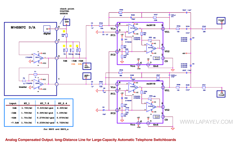

Figure 27. Audio analog compensated output audio driver 3.1 Ultralinear Hi-Fi Preamplifier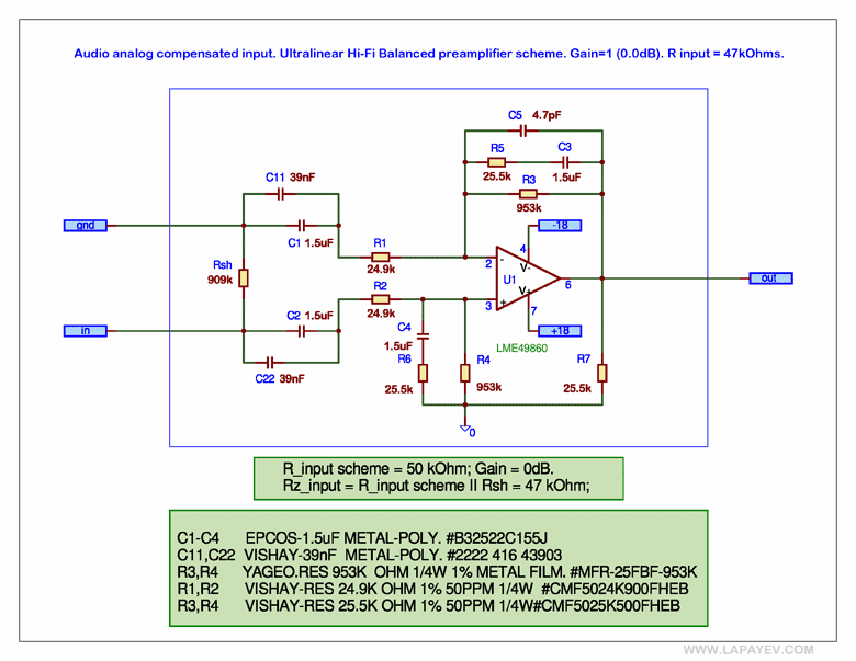
Figure 28. Audio analog compensated input. Ultralinear Hi-Fi preamplifier scheme And now we'll talk about Hi-Fi. It is known how important and often conflicting the requirements to the input cascade of a high-quality amplifier are. On the one hand, you should provide a wide frequency band and on the other hand you shouldn't let anything unwanted pass. You should find a compromise. Figure 28 shows a practical scheme of a balanced high-end audio preamplifier built with the use of the compensation principle described above. Frequency and phase response in the operating part of the band have a smooth characteristic. See Figure 29. In infrasonic frequency range, preamplifier frequency response falls sharply thus blocking the unwanted noises of infralow frequency at the scheme input. Input impedance is 50 kOhms, quieting sensitivity is 0dBu, voltage gain is 1.0 in the whole operating frequency band. Frequency response deviation in the 1Hz - 1kHz frequency band is not higher than 0.06dB. A small high-frequency cut is caused by only blocking capacitor C5 and can be compensated easily if needed. Thus, the present scheme using high-quality film input capacitors of a small nominal value - 1.5μF has quite high frequency and phase response parameters. When OpAmp LME 498xx is used, THD level doesn't exceed 0,0001% (-120dB). But I think the scheme is ultralinear and has excessive capacity in the lower part of the frequency band. If it is not necessary, it is better to narrow the frequency band in the lower part. The scheme with a narrow pass band in the lower part of frequency range is shown in Figure 30. 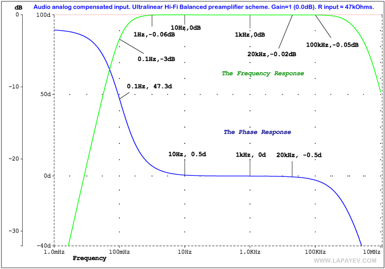
Figure 29. Audio analog compensated input. Ultralinear Hi-Fi preamplifier. Frequency and phase responses 3.3 Ultralinear Hi-Fi Preamplifier with Rumble Filtering
Interesting fact.Vented speaker system and passive radiator speaker system take a leading position on the world market of speaker systems. According to some reports, they amount to 80% of the total small and medium class speaker systems production. When using such speaker systems, you should always remember that the loudspeaker becomes completely undamped and enters piston action mode at frequencies lower than those of vent (or passive radiator). At this point, the loudspeaker will behave as if it has no baffle. But the loudspeaker isn't designed for that and it can lead to its physical destruction. On the contrary to the sealed box speaker system, where the loudspeaker winding would burn out rather than its cone gets broken. 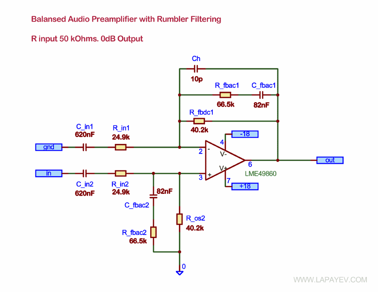
Figure 32. Audio analog compensated input. Ultralinear Hi-Fi preamplifier with a rumble filtering scheme That's why when the amplifier works with a vented or passive radiator speaker system, you should always limit the ultralow part of the audio range to protect the loudspeaker from destruction. It's better to do it quite sharply but with care in order not to limit the level of wanted low frequencies and not to distort the signal phase, which is quite contradictory. The scheme of such preamplifier is shown in Figure 32. It's a practical scheme of a balanced high-end preamplifier with rumble filtering. 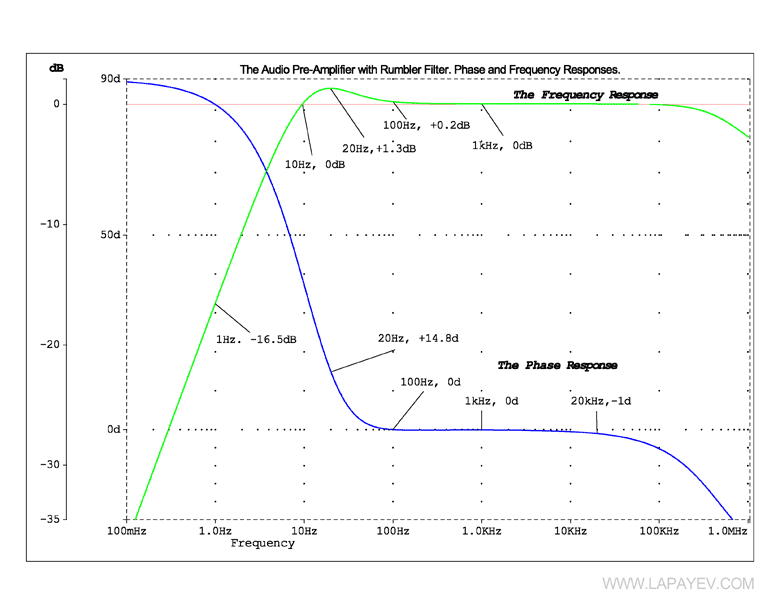
Figure 33. Audio analog compensated input. Ultralinear Hi-Fi preamplifier with rumble filtering. Frequency and phase responses As you can see in Figure 33, the scheme frequency response has a slight increase in the low frequencies band (about +1,3 dB), and then it falls and has the same rejection level as in Figure 30 of about 6dB per octave. Phase response, on the contrary, has a smooth characteristic. The method was described in detail on page 13 (Figure 10, 11). A slight increase at the end of low-frequency band doesn't spoil the sound or cause muttering but rather raises SPL at wanted frequencies, helping small and medium class speaker systems, which vent adjustment frequency is usually about 30Hz or higher. This is perhaps my favorite scheme in its class. I make a good use of this principle in my current business projects. 3.3 Linear Audio DriverNow it's turn of practical output analog schemes. Figure 37 shows a high-quality audio driver designed for a low-resistance load of 600 Ohms. Cascade voltage gain is 1.0, low cutoff frequency on 3dB level is 5Hz. The scheme contains only high-quality film capacitors of small capacity. Figure 38 shows frequency and phase responses of the present scheme. 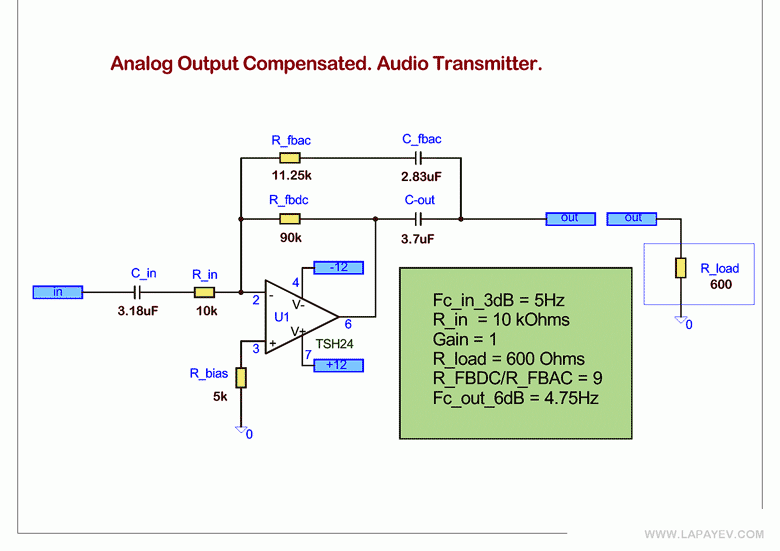
Figure 37. Audio analog compensated output scheme. 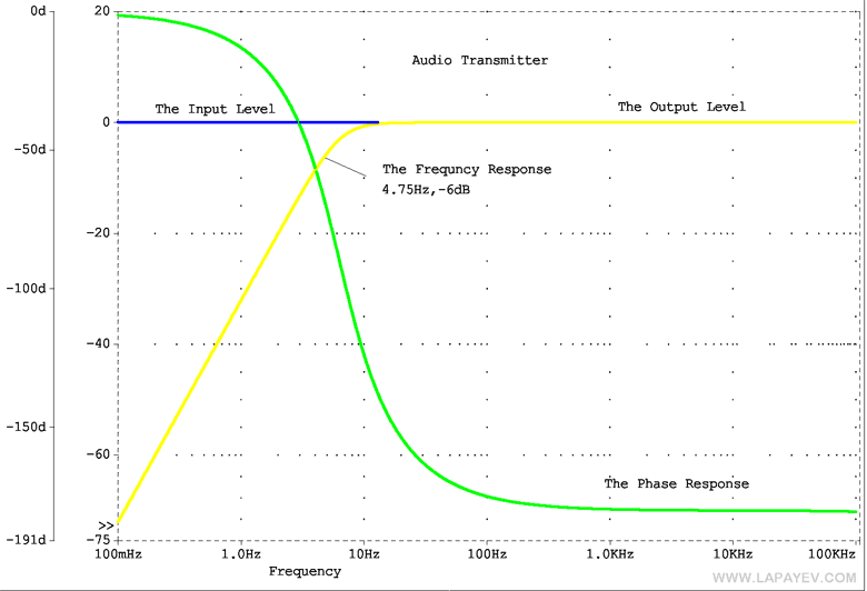
Figure 38. Audio analog compensated output. Frequency and phase responses 3.4 Linear Video DriverFigure 39 shows the example of a video driver scheme designed for a standard load of 75 Ohms. The gain equals to 1.0, lower peak frequency range at -3dB level equals to a half-frame sweep of 60Hz. The scheme contains only high-quality film capacitors of comparatively low capacity. Figure 40 shows frequency and phase responses of the given scheme. 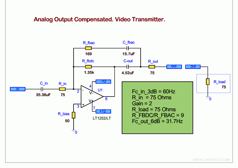
Figure 39. Video analog compensated output scheme 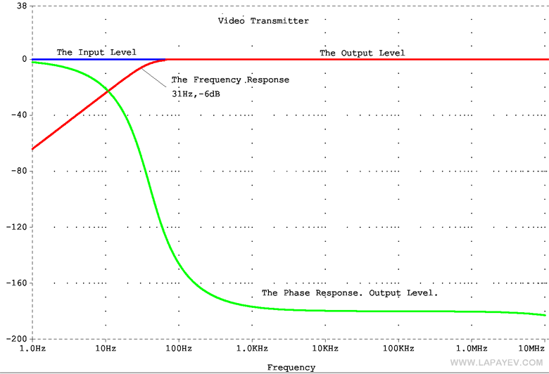
Figure 40. Video analog compensated output. Frequency and phase responses 3.5 Ultralinear Balanced Audio Phones DriverLet's take a look at one more type of an audio driver working with a precise line match. It is a bidirectional analog audio scheme with an input hybrid system (not shown in the figure) loaded on a bidirectional pair line. In addition to the desire of having the maximum linear frequency and phase responses, there is one more quite important requirement - the output part of the scheme must have zero impedance in the whole range of operating frequencies. In this case, the scheme output impedance will depend only on series resistor at driver output, and the cascade will perfectly match the opposite load, and the hybrid system will perfectly split input and output signal flows. Figure 41 shows such a scheme. 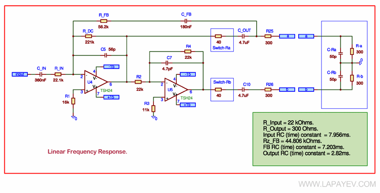
Figure 41. Ultralinear balanced audio phones driver compensated scheme. R input 20 kOhms, R output 300 Ohms. R load balanced 600 Ohms. As we can see in Figure 41, the scheme has a balanced output and is composed of direct and inverse channels loaded on the line through analog switches (Switch Ra and Rb). For example, we choose 40 Ohms impedance for open switches. The gain is 1.0. The output impedance is 300 Ohms. Figure 42, 43 show frequency and phase responses, and Figure 44 shows inverse current inflowing into driver at line input signal voltage 1V/RMS. The given scheme has the following advantages:
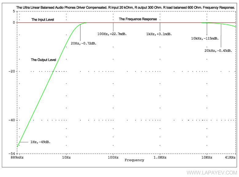
Figure 42. Ultralinear balanced audio phones driver compensated. Frequency response 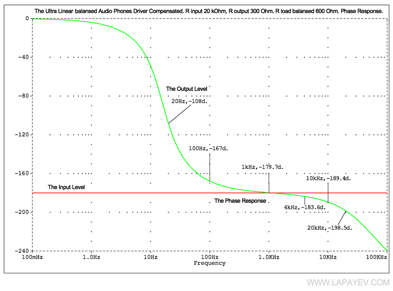
Figure 43. Ultralinear balanced audio phones driver compensated. Phase response
Interesting fact.Everyone knows that during analog audio signal transmission there is a real problem with noises of industrial power grid frequency and their harmonics. The given scheme has a good ability of common mode rejection while using hybrid system for input signal processing. This is possible thanks to consistency of driver output impedance (which is also input impedance for the input signal) in the entire operating frequency range including its lower part. 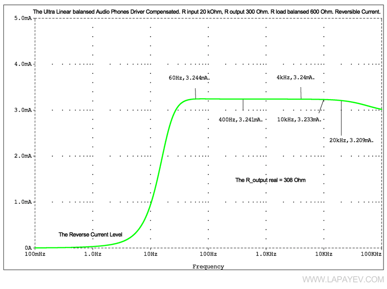
Figure 44. Ultralinear balanced audio phones driver compensated. Reverse current As you can see in Figure 44 the scheme has good constant output impedance in the entire operating frequency range, which equals to 8 Ohms. It makes this scheme easily adaptable to the line impedance factor and to the opposite load by standard means of switching the series resistor at output. 3.6 Linear Balanced Audio Driver With Low-Pass 44kHz Filter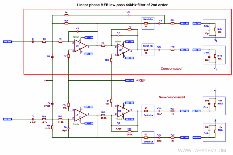
Figure 45. Linear balanced audio driver with low-pass 44kHz filter scheme Let's take a look at another interesting scheme. It's a high-class balanced audio driver designed for a 10 kOhm load. See Figure 45. For comparison, the upper channel is built according to the principle of compensation, and the lower one is built according to the principle of standard circuit design. For example, output capacitors of both channels have the same nominal values. The gain equals to 0 dB. The scheme contains a low-pass act filter of the second order with the cutoff frequency of 44 kHz. The resulting frequency and phase responses of the upper channel are shown in Figure 46 and 47, and Figure 48 shows GDT. Due to commercial reasons, passive elements nominal values are not shown on the scheme. 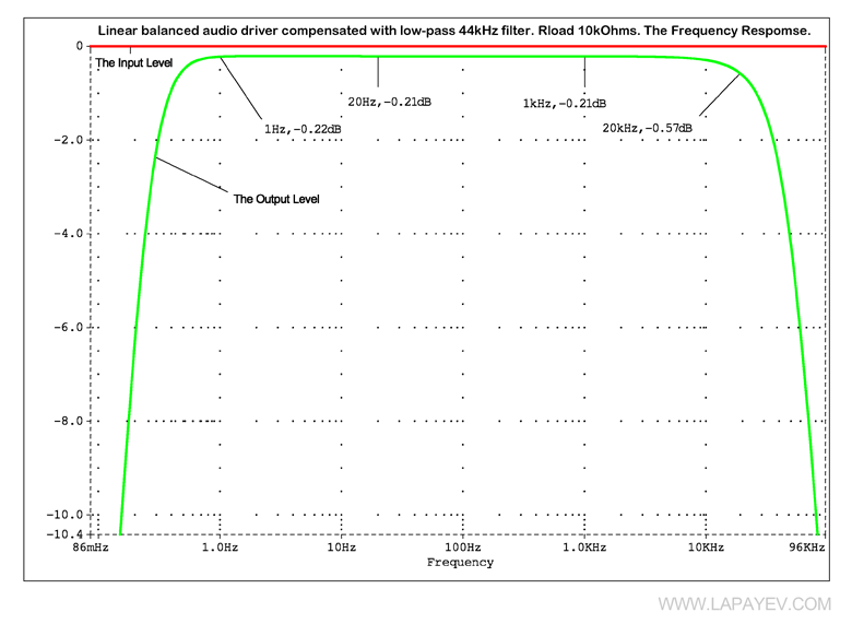
Figure 46. Linear balanced audio driver with low-pass 44kHz filter. Frequency response 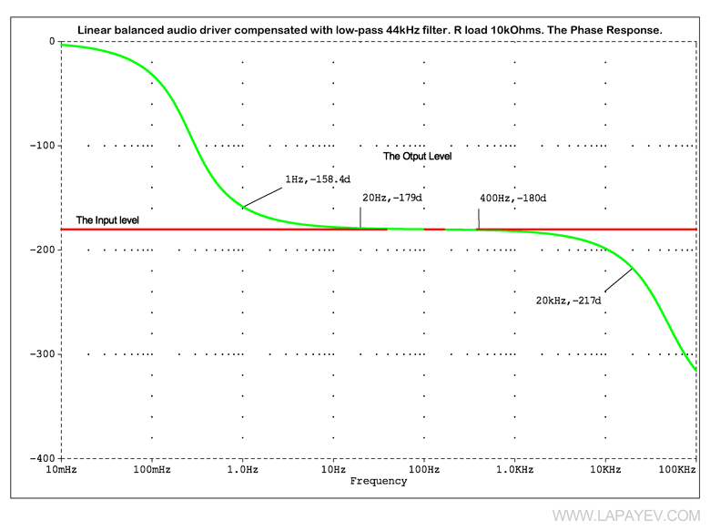
Figure 47. Linear balanced audio driver with low-pass 44kHz filter. Phase response The driver is loaded on the line through a quite cheap 74HC4066 analog switch. The best representatives of this class have transfer impedance of not less than 30 Ohms, and the THD level is not better than 0.05% (as a rule both of them are worse). Also diode (antistatic) protection and cheap output electrolytic capacitors are used, which also doesn't make the output signal more linear. Earlier, all this resulted in the overall level of THD of more than 0.2%, which was quite notable in the low-signal range. After applying the principle of compensation, the THD level became not more than 0.007% in the whole audio frequency range. Moreover, the scheme is simple and does not have expensive parts. No doubt that it is nice to take a look at the diagram in Figure 46. 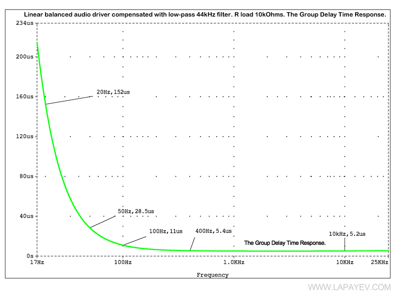
Figure 48. Linear balanced audio driver with low-pass 44kHz filter. Group delay time response 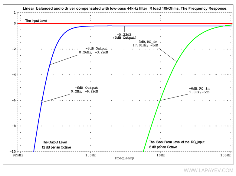
Figure 49. Linear balanced audio driver with low-pass 44kHz filter. Frequency response comparative characteristics For comparison, Figure 49 shows low-frequency parts of the frequency response of high (compensated) and low (standard) channels in detail (Figure 45) at equal input and output impedance values. The difference is clear not only in the level of low operating frequency range, but also in linearity of the frequency response in its lower operating part, and in steep roll-off of its response at the cutoff frequency (6dB and 12dB). 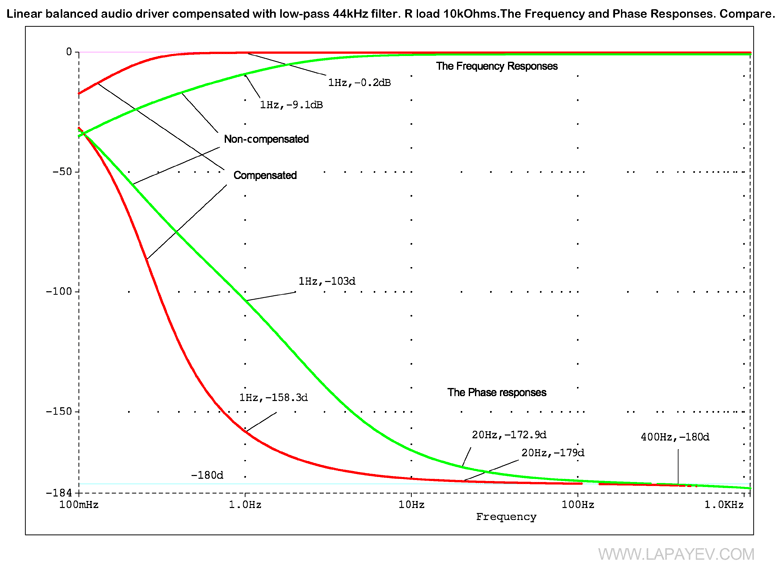
Figure 50. Linear balanced audio driver with low-pass 44kHz filter. Phase response comparative characteristics Figure 50 shows a combined diagram of frequency and phase responses of high (compensated) and low (standard) channels (Figure 45) with equal input and output impedance values. Diagrams speak for themselves. 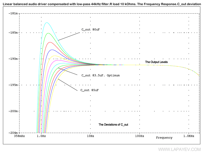
Figure 51. Linear balanced audio driver with low-pass 44kHz filter. Dependence of frequency response level in low-frequency part on output capacitor nominal value And here comes the conclusion. Figure 51 shows several frequency responses of the higher compensated channel with deviations of the output capacitor nominal value from its optimal (design) value. You need to pay attention to the fact that response deviation from the needed level is not so significant, given real variation of capacitors parameters, which makes the usage of the compensation principle commercially suitable, which was proved many times in practice. Hereby let me finish. Should you have any questions or suggestions I'll be glad to hear them. There are more information available in the full version of this article. It includes more detailed calculations, special calculation program, examples and etc. In order to get full version of this article please contact me using this form. |