
Alex Lapayev. Analog Input/Output Compensated....soon everything will be digital, but the ear and tongue will remain analog... Long ago a friend of mine showed me an article about an electronics engineer. When it was time to retire, he spent his savings on an expensive audio system, synthesizers, measuring devices and the like. Having set up synthesizing and measuring equipment in the study, he also set up everything in terms of audio signal processing in the cellar. Thus, a signal of a complicated form was synthesized, sent to the cellar, where it was modified, recorded, reproduced, restored in the form and sent up to be compared with the initial one. The equipment was perfect - both signals coincided on the oscilloscope screen - without distortions. That was nirvana... When I finished reading, my friend told me with a sad smile: "This is what you'll have in the future". Well, it was noticed long ago that a sinusoidal wave view has a magical effect. On second thought... Modern processing of audio and video information is almost completely exposed to digital signal processing, which gets more qualitative and cheaper from year to year. However, input and output circuits often remain analog. A clear analog audio and video signal. Everybody knows what is needed for it. Flat frequency response, small linear and harmonic distortions, and linear or uniformly decreasing phase response. Let's leave the topic on digital signal processing for other publications and talk about simple input and output buffer analog circuits. 
1. Analog Input CompensatedAn audio circuit input capacitor together with input impedance form a high-pass filter, which in its stop band distorts the signal form. I think it's erroneous to consider Fc selection in the range of 10-20Hz a good thing - we've got rumble filter, which prevents the audio signal from infralow frequencies, for example, for vented speaker systems protection. It's commonly known that the ear is sensitive to phase distortions only of mid-band frequency, let's say from 400Hz to 4kHz. Experiments show that in this frequency band a human can hear phase distortion already starting with 10 degrees. But what do we have in the low-band frequency? It's a well-known fact that in this case the ear is hardly sensitive to phase distortion and we can hear no difference. Usually it's true, but we can still hear the out of tune sound but normally at degrees greater than 10. As a result opinions divided. Two ways are possible. The first one is to use high-quality capacitors of small capacity and have phase distortion using rumble filter. The second one is to have flat phase and magnitude in the infralow area by increasing the capacity up to tens microfarads, which involves irreplaceable electrolytic capacitors and this is not good. Especially when working without a DC shift. Though using audio capacitors (for example, ELNA-RFS-35V101MH5#) improves the situation. And still... In the late nineties while developing brand new output analog audio drivers for big telecom stations I faced the following problem. I had to provide linear frequency response working with a long line through capacitors of quite small capacity since electrolytic capacitors couldn't be used due to many reasons. That's when I thought about the idea of frequency response and phase response compensation at low-pass frequency range. I think that high-quality ceramic and film capacitors of small capacity, for example, audio polypropylene should be used, which enables impedance increase compensation with frequency drop using the feedback. Thus we can get almost perfect frequency response and phase response in the low-frequency part of the operating range. That's how the idea to compensate the dependence of audio driver impedance on frequency came to life. Here we should divide negative feedback by voltage into two parts: negative feedback with direct-current voltage (DC) and negative feedback with alternating current voltage (AC). They should be calculated so to reach frequency response cut compensation and phase response change at low frequency. If we need a rumble filter, then a compromise should be made. We will talk about it later. 1.1. Non-Inverted SchematicsThe figure below shows the principle of an input non-inverted analog buffer amplifier or preamplifier with compensated frequency response and phase response. Everything is quite simple as you can see. Negative feedback by voltage is divided into negative feedback with DC voltage (R_fbdc) and negative feedback with AC voltage (R_fbac + C_fbac). To receive maximum linear frequency response in low-frequency part, time constants of input circuit and feedback circuit should be compensated: CR Input Time Constant = CR Feed Back Time Constant It is obvious that when changing input signal frequency, input complex impedance and total voltage gain change synchronously (increasing or decreasing) by one law, compensating frequency response cut and phase response increase in the low-frequency band. Voltage gain on DC should be greater than voltage gain on AC (R_fbdc / R_fbac ratio). This allows the circuit to compensate frequency response and phase response changing total voltage gain according to frequency by a certain law. 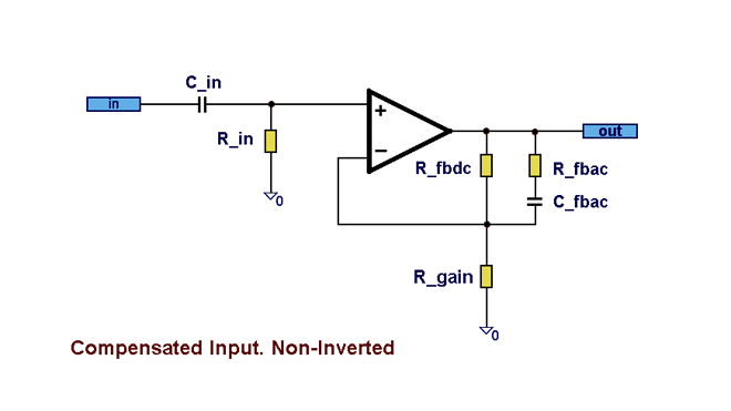
Due to this a small input capacitor is used, which makes it possible to use a ceramic or film capacitor instead of an electrolytic one. If CR_Input Time Constant and CR_Feed Back Time Constant are not equal, phase and frequency responses in low-band frequency will mutually change in the opposite direction, which can be useful. The detailed examples are provided below. 
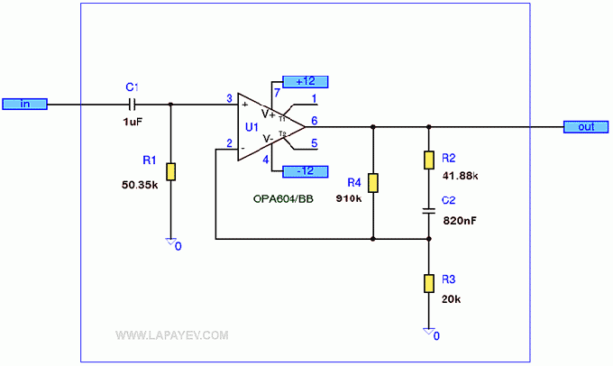
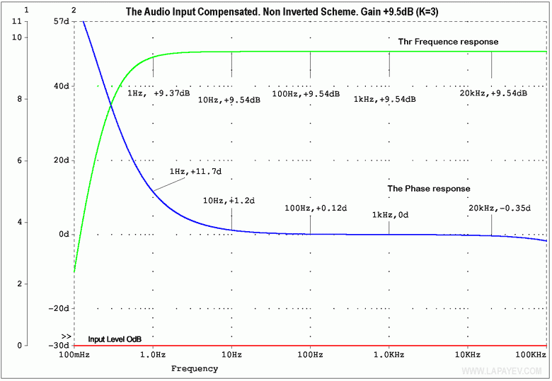
Interesting fact. No matter how high voltage gain of modern operational amplifiers is, it gets down quickly with the frequency increase. As it is known, it leads to a number of frequency and phase response distortions including pulse responses. The mentioned compensation principle requires extra gain from the operational amplifier but only in the most low-band frequency part, where it causes no problems and has no influence on total qualitative scheme indices. Looking ahead, we can see in section 3. Practice some practical schemes with the compensation principle of input and output analog circuits. The scheme in Figure 45 shows output audio driver loaded on the line through a cheap analog switch of 74HC4066 type. The best representatives of the class have 30 Ohms resistance and THD level not less than 0.05% (usually they both are lower). Diode (antistatic) protection is used together with cheap electrolytic capacitors. Earlier it led to THD level higher than 0.2%, which was mostly noticeable in low-signal frequency. After compensation, THD level became not higher than 0.007% in the whole audio frequency band. The scheme is simple and has no expensive parts. Figure 01 shows the scheme of an input non-inverted amplifier with compensated amplitude and phase responses. Gain = 3 (+9.5dB). Figure 02 shows phase and frequency responses. Main ratios are: 
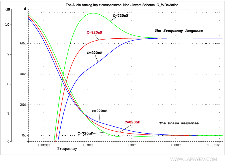
C (μF), R (kOhms), CR time constant (ms). Figure 01. Audio analog compensated input. Non-inverted scheme. Gain = 3 Negative feedback by voltage is divided into two parts: negative feedback with DC (R_FBDC - R4) and negative feedback with AC (RC_FBAC - R2C2). CR_Input Time Constant = CR_Feed Back Time Constant. Figure 03 shows the dependency between phase and frequency responses on the accuracy of this formula. As you can see, input impedance is 50 kOhms and capacitor capacity is only 1μF at the scheme input, which allows for a high-quality capacitor, for example, a polypropylene instead of an electrolytic one. Phase response became more linear; phase distortion at 10Hz is just 1.2 degrees. Fc (-3dB) decreased significantly to 0.2 Hz. See Figure 02. If using a standard scheme with the same nominal values of R1 and C1, Fc would be as follows: 
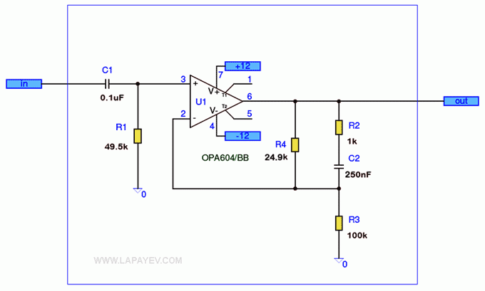
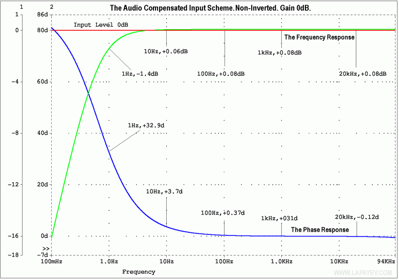
Figure 02. Audio analog compensated input. Non-inverted scheme. Gain = 3. Frequency and phase responses Figure 03. Audio analog compensated input. Non-inverted scheme. Gain = 3. C_fb deviation. Frequency and phase responses Figure 04 shows one more scheme of an input non-inverted amplifier with compensated amplitude and phase responses. Gain is about 1 (Gain = 0.065dB). It should be noted that it seems impossible to get exact gain voltage equal to 1 using this scheme. Input capacitor is only of 0.1 μF capacity. Figure 05 shows phase and frequency responses. The main ratios are the same as in Figure 01. Figure 04. Audio analog compensated input. Non-inverted scheme. Gain = 1 Figure 05. Audio analog compensated input. Non-inverted scheme. Gain = 1. Frequency and phase responses 
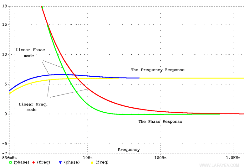
Interesting fact.If we add Kph coefficient to the formula for calculation of capacitor C2 nominal value basing on the graphics from Figure 03, as it is shown below, output phase response will get more flat in the low-frequency part and become almost linear in calculations. Frequency response gets a slight increase (about 1dB) in the low-frequency part, which doesn't interfere and even can be useful. See Figure 06. 
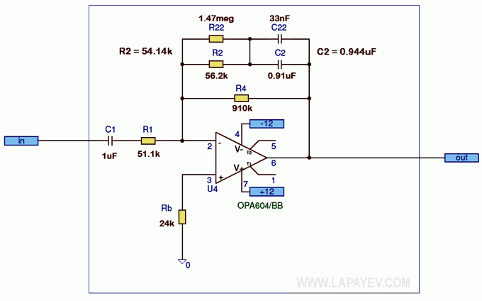
Figure 06. Audio analog compensated input. Non-inverted scheme. Linear phase and linear frequency responses 1.2. Inverted SchematicsIn this section we'll focus on the principle of analog signal magnitude and phase compensation in low-frequency part as applied to OpAmp inverted switching. The example is shown in Figure 07, 08, 09. I think this scheme is more preferable for using compensation principle than the scheme of inverted amplifier first of all due to its simplicity. When calculating, we need just to make the input circuit CR time constant and the feedback circuit CR time constant equal as well as tie them up to the voltage gain cascade. Main ratios are: 
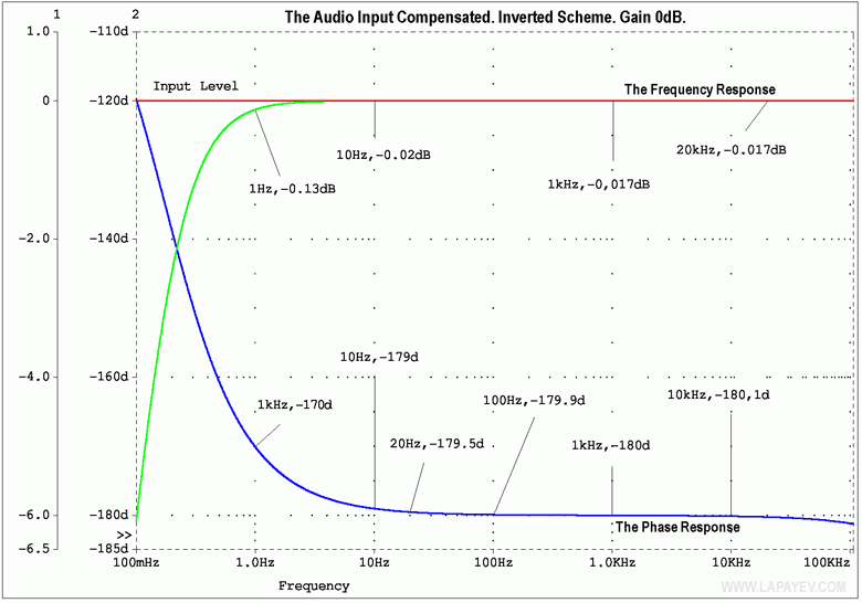
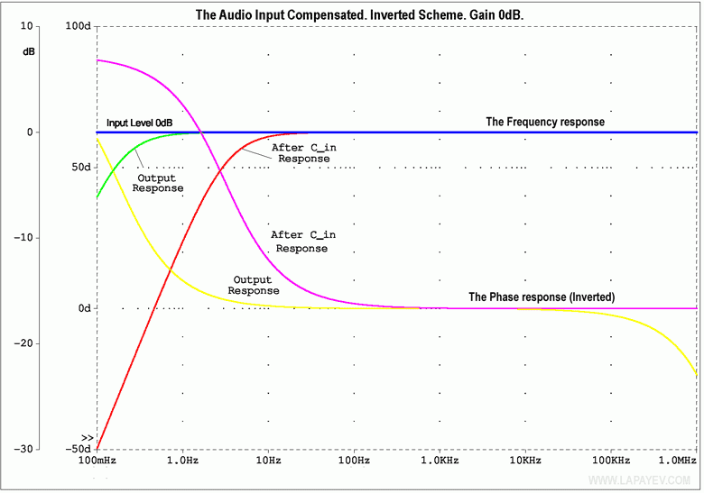
Figure 07. Audio analog compensated input. Inverted scheme. Gain = 1 Figure 08. Audio analog compensated input. Inverted scheme. Gain = 1 Figure 09. Audio analog compensated input. Inverted scheme. Gain = 1. Main diagrams of input, output signal dependencies, and C_input signal. The diagrams show the principle of compensation The input capacitor has a relatively small nominal value of - 1μF, which allows for a high-quality polypropylene capacitor instead of an electrolytic one. Input impedance is 50 kOhms. Phase and amplitude responses got linear in the lower part of the band, and low work frequency moved far to the left side of the diagram. Figure 09 shows comparative characteristics of signal magnitude and phase before and after an input capacitor is used and right at the scheme output. 
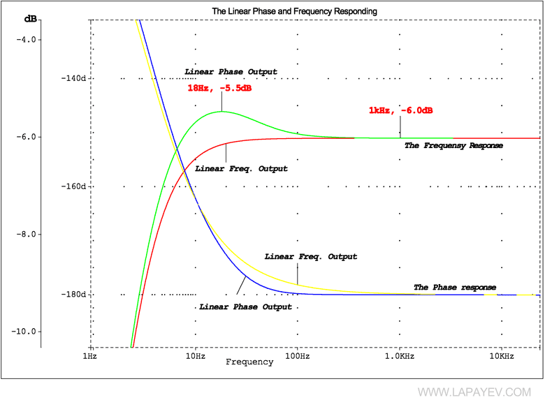
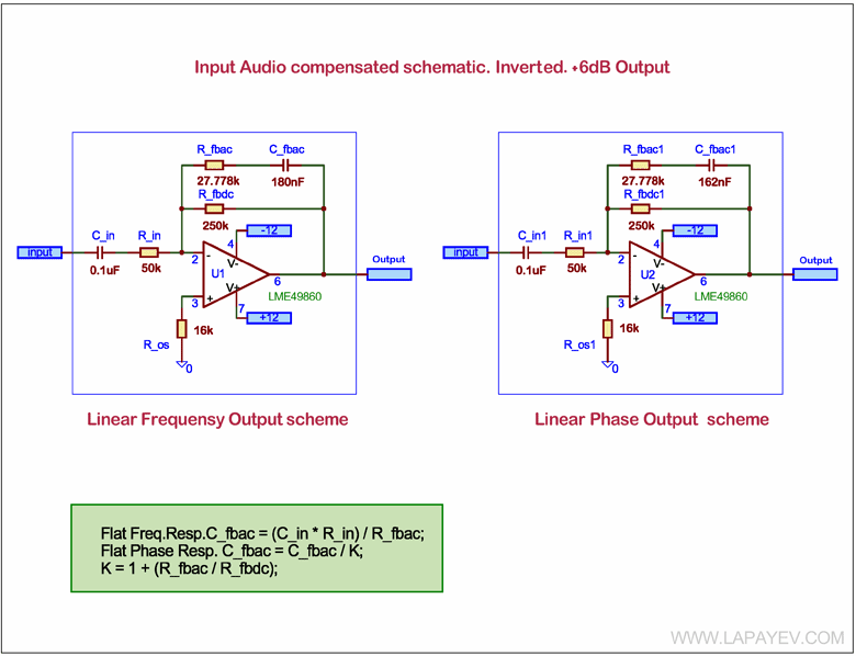
Interesting fact. Likewise in the case of non-inverted amplifier (page 9), if Kph coefficient is added to the calculation formula of C2 capacitor as it is shown below, then output phase response will get maximum flat in the low-frequency band, and become almost linear in calculations, while frequency response will get a little increase in the most low frequency band. See Figure 10, 11. 
Figure 10. Audio analog compensated input. Inverted scheme. Gain -6dB. Diagrams of dependencies of output signal in linear phase mode and linear frequency response Figure 11. Analog compensated input. Inverted scheme. Gain +6dB. Schemes of linear phase and linear frequency response There are more information available in the full version of this article. It includes more detailed calculations, special calculation program, examples and etc. In order to get full version of this article please contact me using this form. |
