
Alex Lapayev. Analog Input/Output Compensated.2. Analog Output Compensated SchematicsThis chapter describes circuit design of output analog schemes. It's getting more complicated and challenging, as there are lots of problems with qualitative analog audio and video outputs. For example, it refers to widely used output consecutive analog switches that bring noticeable harmonic distortions. Or diode, or varistor protection, which is also far from being harmonic. Moreover, there is a specific problem with the way an output analog driver works at low-resistance load. It relates to professional audio and video systems, radio devices, audio used in high noise conditions, audio and video automotive, video drivers and transmitters, etc. As a rule, typical load impedance bogey is 75/150/300/600 Ohms. There's always a good reason to increase the capacity of output capacitors to infinite limits when operating at low-resistance load. As a minimum, you need to increase it up to tens of microfarads in order to get rid of signal phase and magnitude distortion at output. It's quite obvious that to achieve this, irreplaceable electrolytic capacitors are used again. Unfortunately, they bring their notable contribution to high noise and distortion increase in the output signal. Quite often you have to confine yourself to the capacity of 5-50 microfarads simply because of their size. Sometimes you simply cannot use electrolytic capacitors in radio devices due to line DC voltage reversal and also due to their low reliability. It's a problem to solve. Let's use the principle of magnitude and phase compensation in this case. See Figure 12. 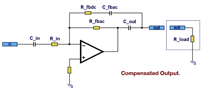
Figure 12. Analog compensated output principle So the schemes considered earlier had two initial time circuits each (CR time constant) - RC_INPUT and RC_FB, now we have one more connected with a C_out output capacitor. Now it's not that easy to calculate scheme parameters, because, firstly, C_out capacitor is loaded at complex circuit impedance consisting of R-load, C_FBAC and R_FBAC, and, secondly, the amplitude of input exciting voltage for an output circuit (OpAmp output) is not frequency harmonic and depends on several factors simultaneously. See Figure 13, 14. 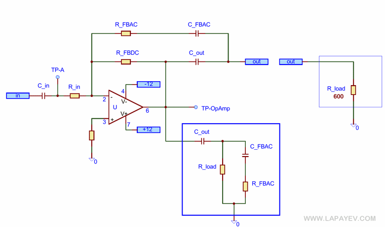

Figure 13. Analog compensated output. Output CR time constant. Equivalent scheme 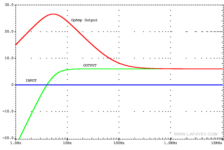
Figure 14. Analog compensated output. Gain = 2. Main dependencies of input, output voltage and OpAmp output Figure 14 based on output driver example (Gain=2) shows how output voltage OpAmp compensates C_out reactive impedance depending on the frequency. The more Gdc (Rfbdc / Rfbac) ratio is, the better it is for compensation but the worse for the scheme dynamic range. For example, with the amplification coefficient of 6dB, the output voltage peak OpAmp will reach 26dB (frequency 5-6 Hz). In other words, if the maximum level of the input signal is 0 dBu (0.776 V/rms, 1.095/amp, 2.191V/p-p), then the output will have 4.382V/p-p, and OpAmp output will have 4.382V/p-p at its maximum point! It means that the voltage level +/- 22V will be at its limit. (Not considering OpAmp real output characteristics). You should always remember this when using this schematic solution. 2.1. Main Ratios
Figure 15 shows the practical scheme of an output analog audio driver. The calculations are made according to the formulae shown above. The scheme upper channel is built on the principle of compensation, while the lower one - according to the standard scheme. For a relatively simple characteristics comparison, nominal vales of input and output capacitors and CR time constants correspond to one another on both schemes. R_input = 50 kOhms, Gain=1, Fc_6dB=5.1Hz. The capacity of input and output capacitors is comparatively small (0,51μF and 0,33μF). You can easily do without electrolytic capacitors. Figure 16 shows the dependency between the following signal levels:
The comparative diagrams of frequency and phase response of compensated (RED) and standard (BLUE) schematics are shown in Figure 17. 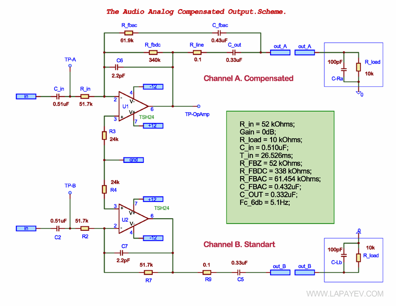
Figure 15. Audio analog compensated output. Gain = 1. Comparative scheme of compensated and standard schematics Figure 16 clearly demonstrates how OpAmp output voltage compensates reactive and resistive impedance of the output circuit (C_out + R_line). Frequency response gets notably flat in the low-frequency band and steeper in the stop band. The attenuation is 11-12dB per octave instead of 6 dB. The details are shown in Figure 17. 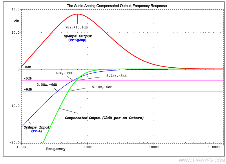
Figure 16. Audio analog compensated output. Gain = 1. Main dependencies between signal levels: after input capacitor (TP-A), OpAmp output (TP-OpAmp) and driver output (OUT_A) 
Interesting fact.Important! The scheme is very stable when operating at a reactive load, as the output series resistor R_line has minimum influence on the scheme output characteristics. Thus, resistance can be increased up to the desired level during the driver work at a reactive (for example, capacitive) load. You should also note that one more asset of the schematics principle is the harmonic and linear distortions sum compensation, which is caused by the driver output circuit. As it is known, such schemes outputs often use antistatic protection (diode or varistor) or analog switches that cause quite a high level of harmonic distortions. Output capacitor, usually electrolytic one, in its turn causes a number of distortions including harmonic ones. The scheme provided allows compensating distortions almost completely and clearing the input signal from them. 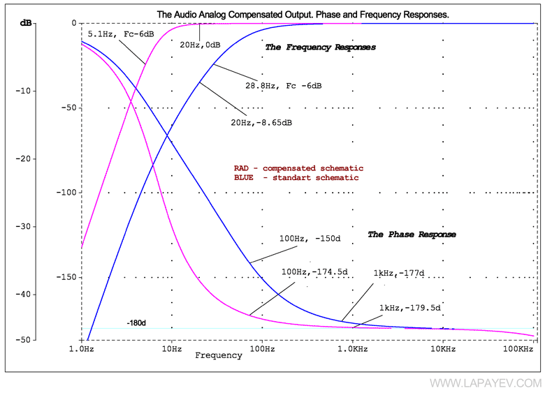
Figure 17. Audio analog compensated output. Gain = 1. Phase and frequency response of compensated (RED) and standard (BLUE) schematics. Comparative diagrams However when using analog switches, which disable driver output load (R_line on the scheme), you should always remember that the feedback circuit always remains connected to the load (R_fbac and C_fbac). This may cause an unwanted, though small enough signal in the load, since the scheme becomes disbalanced in the out-of-load mode. Since R_fbac is much higher than R_load and just several times lower than R_fbdc, the level of acquired distortions is nearly missing. The best way in this case is to switch off the driver input together with the driver output, which can be done by delivering zero potential to the scheme input. 2.3. SupplementIt is fair to say that maximum linear frequency response in the low-frequency part of band has two C_out values with constant scheme parameters. It means that C_out equations have two solutions. The first value (Small Capacitor) is used mostly in practice and is shown in calculations while the second one (Large Capacitor) has a greater nominal capacity value and I think has no practical usage. That's why we'll skip calculations and theory related to this topic. Figure 18 shows the scheme of the output driver, the upper channel of which is built with C_out high nominal value - Large Capacitor while the lower one with low nominal value - Small Capacitor. 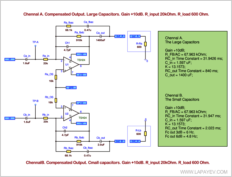
Figure 18. Audio analog compensated output. Gain = 10dB. Comparative scheme of C_out large and small nominal values Capacitors nominal values differ greatly - 2.0μF and 1400μF. Figure 19 shows frequency and phase response diagrams with the use of Large Capacitor and Small Capacitor. It is clearly seen that scheme characteristics with the nominal value of 1400μF are shifted far in the low-frequency part of the band. Though it should be noted that in practice you can get such frequency and phase responses if the whole scheme of compensated output driver is calculated wisely using C_out small nominal value (Small Capacitor). 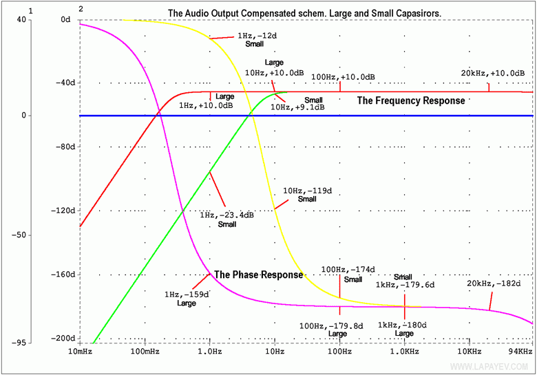
Figure 19. Audio analog compensated output. Gain = 10dB. Comparative schemes of C_out small and large nominal values. Frequency and phase responses. Small and larges capacitors modes. Comparative diagrams 3. ComparisonI would like to spend some time to describing the main characteristics of 3 main types of the given schemes. Let's describe the above-mentioned types as follows:
Figure 20. A,B,C show examples of the given types of schemes. Figure 21 shows their frequency response and phase response. To make it look clearer, such parameters as time-setting circuits of input circuits (CR time constant), input impedance, gain and FBDS/FBAC ratio are shown equally for all examples. 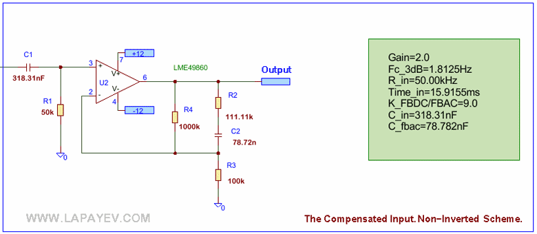
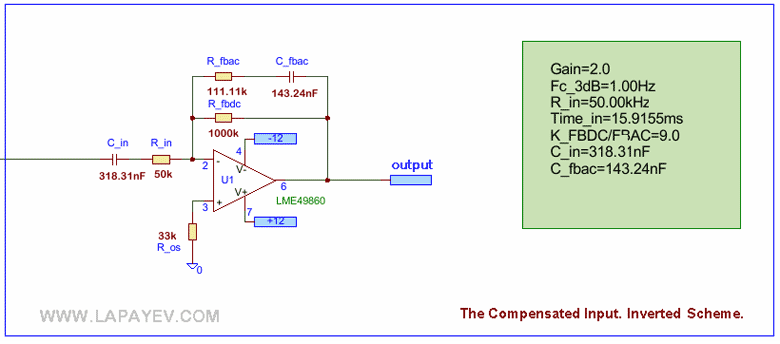
Figure 20. A,B,C. Audio analog compensated inputs (inverted and non-inverted) and output schematics at equal input CR time constant parameters It's obvious that the first two types of schemes (Compensated Input) with one RC circuit each behave as high-pass filters of the first order and have 6dB octave attenuation. While having equal initial parameters (CR time constant of input circuits, R-input, gain and FBDS/FBAC ratio) the inverted scheme has got better phase and amplitude response against the non-inverted scheme. The third type of scheme is Compensated Output, which has two RC-circuits, behaves as a high-pass filter of the second order, and has 12dB octave attenuation. FC and linear part of phase response are moved to the right along the frequency response line. For comparison: Fc Inverted Scheme=1Hz, Non-Inverted Scheme Fc=1.8Hz and Compensated Output Scheme Fc=12.3 Hz. 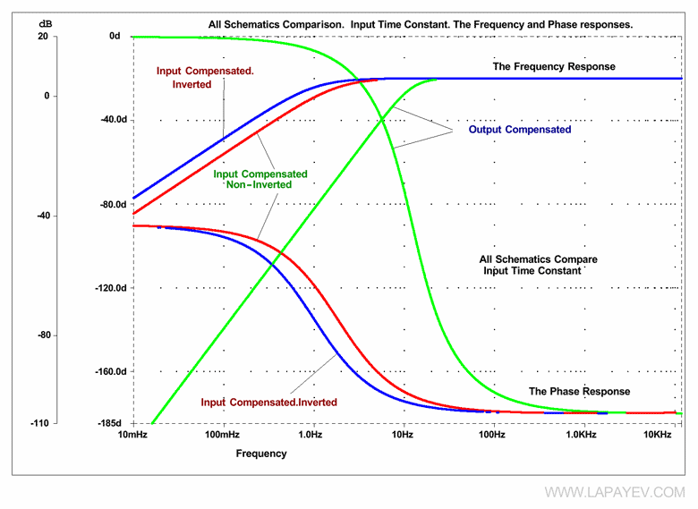
Figure 21. Audio analog compensated inputs (inverted and non-inverted) and output schematics. Comparative characteristics of frequency and phase responses with equal parameters of input CR time constant Having come to a conclusion of the above-mentioned comparison, it would be interesting to take a look at the behavior of the given types of schemes at more or less equal Fc cutoff frequencies. Figure 22. A,B,C show schemes with theoretical Fc cutoff frequency at about 1Hz. Figure 23 shows their amplitude and phase responses. It's clear that at comparatively equal Fc, the non-inverted scheme has twice higher CR time constant of input circuit than the inverse scheme, and compensated output scheme has a 10 times higher one. At equal input impedances, it will require the corresponding capacity increase of the input capacitor, which is not always wanted. But it needs to be specified that the type of scheme described as Compensated Output in general has a different purpose than the schemes of input compensation. 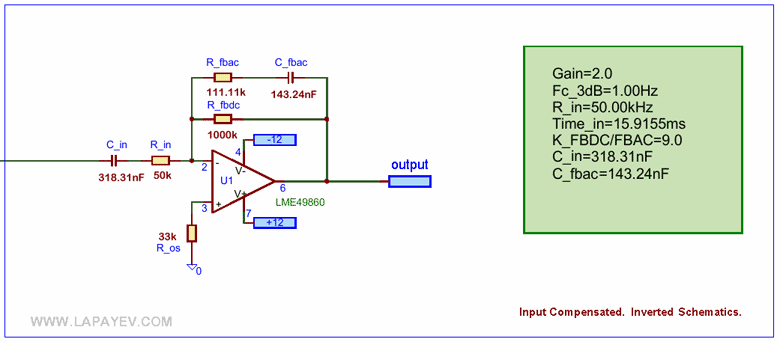
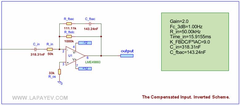
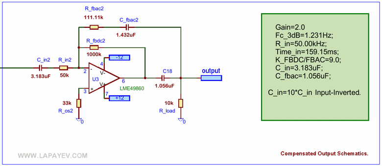
Figure 22. A,B,C. Audio analog compensated inputs (inverted and non-inverted) and output schematics at equal Fc parameters 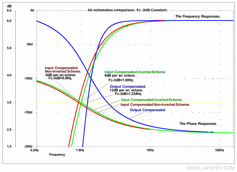
Figure 23. Audio analog compensated inputs and output schematics. Comparative characteristics of frequency and phase responses at equal Fc parameters Now let's talk about dynamic features of the given schemes. Figure 24, 25 show examples of pulse (transient) responses. It's quite expected that schemes of the first order (Compensated Inputs) have better pulse responses than schemes of the second order (Compensated Inputs and Output), which have quite similar responses with Chebyshev filter of the same order. The main difference is that the main purpose of the output compensation is to get maximum linear frequency response in the operating field, and it's known that the purpose of the Chebyshev filter is the maximum steep response of cutoff frequency. See Figure 26. 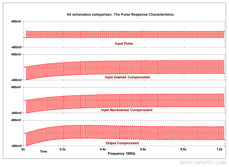
Figure 24. Audio analog compensated inputs and output schematics. Comparative pulse responses at equal Fc parameters (about 1Hz). Meander, frequency 100Hz 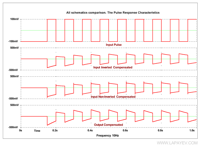
Figure 25. Audio analog compensated inputs and output schematics. Comparative pulse responses at equal Fc parameters (about 1Hz). Meander, frequency 10Hz 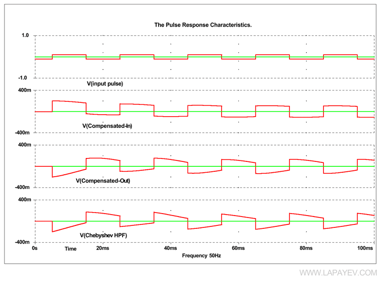
Figure 26. Audio analog compensated input/output schematics and Chebyshev high-pass filter of the second order. Comparative dynamic characteristics at equal Fc parameters (about 1Hz). Meander, frequency 50Hz Hereby we finish the massive theoretical part devoted to the method of compensating the low frequency part of frequency and phase responses of input and output analog driver schemes. Further on, we will see the most interesting part - applied real-life working schemes that use the above-mentioned principles. There are more information available in the full version of this article. It includes more detailed calculations, special calculation program, examples and etc. In order to get full version of this article please contact me using this form. |